Introduction of Nanotechnology
Technology with its great advance in the 21st century has enormously widespread roots worldwide ‘Nanotechnology’ the emerging technology of the 21st century surprisingly has created a great impact on our lives today.
Nanotechnology not only involves modern Science but also expands its fields to technologies, Engineering and Mathematics. Nanotechnology is believed to have rapid and strong growth in the coming future.
What If we talk about exponential technology ‘Nanotechnology’ which is defined as the understanding and the control of matter lies in dimensions 1nm to 100 nm.
Thus, throughout history, humans have had exposure to nanoparticles. The concept of the Nanometer was drawn for characterizing the size of particles or collides.
Thus, the use of “nanotechnology” was done firstly to explain the process of semiconductors that occurred in order of Nanometer used for processing, separating, consolidating and deformation. It was the idea of Feynman’s, K.E. Drexler who advanced the idea of “molecular Nanotechnology”. In 1986 he postulated the concept of using nanoscale for molecular structures to demonstrate an act of activation of synthesis of larger molecules.
What is Nanotechnology?
From the word we get the clue that, Nano means ‘very small in size’ If we talk about the size of a Nanometer which is 1nm=10^-9m which is around 100,000 times smaller than a human hair. Nanotechnology is an anticipated manufacturing technology which has inexpensive control. Also, It is referred to as Molecular Nanotechnology which means “a place for every atom and every atom in place”. The excitement among youths and young minds incurred to innovate their creative ideas to make incredibly small scale things is called Nanotechnology which is the fast-moving technology of today’s world. It targets to enable the use of new approaches and materials to build up through nanoscale devices at the nanoscale level.
Scientists today are trying to make the best use of nanotechnology as they rearrange the atoms of an object in a way to create something new, acquiring new properties.
Some of the companies that use Nanotechnology in India are Hexorp (manufacturer of graphene products), Adnano technologies, Bilcare, Mittal Enterprises in Hyderabad etc.
Nanotechnology Exposure to the Future of the 21st Century:
The remarkable industrial applications and exponential growth hype the technological advancements in different sectors like pharmaceutical companies practising and created a great impact on medical equipment like drug delivery and gene therapies also tried in conditions like cancer, diabetes and viral infections.
The food packing industry and cosmetics industry were not far from the improvement in their production. From checking the bacteria activity in food to installing food sensors for safeguarding the quality of the food served helped to make the technology certified by the young minds.
Nanotechnology can be far more used than medicine, showcasing its creation of “nano muscles” to make dolls that could react to a sound by moving eyes, fascinating others through their dynamic actions.
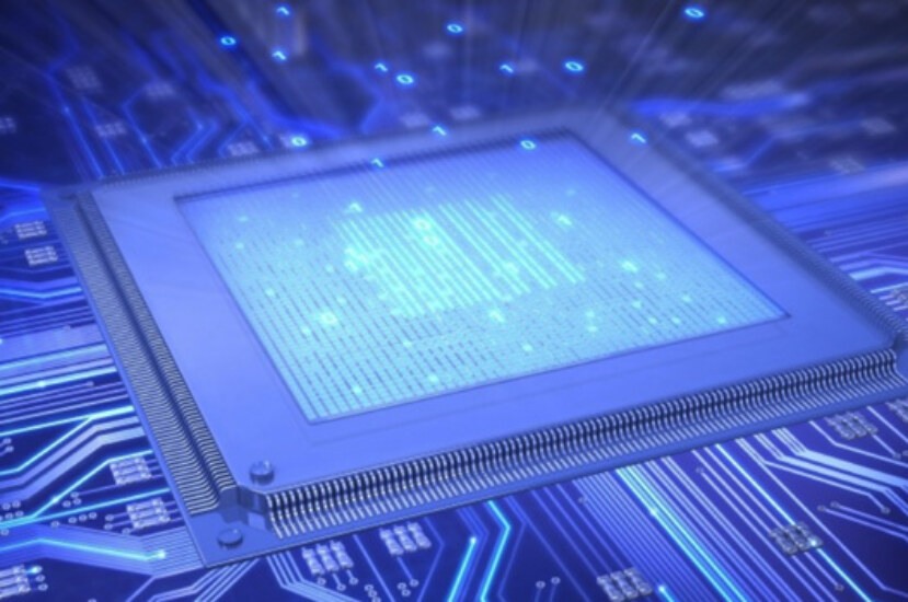
HOW DOES NANOTECHNOLOGY DERIVE NANOELECTRONICS APPLICATION?
ELECTRONICS is an enabling technology which can be said in the simple sense as ‘engineering of tiny machines’ which is potentially impacted from chip making, extending its ways to material to devices, to develop a system-level architecture. It is based on the working of electronic components, and transistors using mainly carbon nanotubes and nanowires. The applications such as computing and electronic products like flash memory chips, the casting of cell phone fabrication of future electronic devices on nanoscale technology with increasing requirements in performance, cost, functionality, advancement, portability and comfortness the microelectronic industry drive its way into the nanoworld of electronics searching for different alternatives to replace the silicon.
The industry was fascinated with the carbon nanomaterials such as (ID) one-dimensional carbon nanotubes and 2D materials like graphene which were the most promising materials for the industry due to their faster and superior electrical properties of fabrication power-efficient electronics. Nanotechnology uses the widest application NANO, OLED, used in quantum computers. The material and devices used in Nanotechnology are so small that the quantum mechanical and interatomic interactions of such materials are learnt extensively.
Nanoelectronics covers a diverse set of materials and devices which share the common characteristics of being so small that their inner physical characteristics i.e. their atomic interaction inside and the quantum role in the mechanical properties play a very significant role in the manufacture of Nanoelectronics.
A report draws a wide range of interest from scientists which outlines the science and engineering community in the UK and abroad. The report likely mentions the next 15 years of development in nanoengineering and measurement, nanomaterials, bionanotechnology, electronics and optoelectronics. The report gives major consideration to issues related to health, safety, environmental and social issues that would arise in these fields.
Various electronic devices manufactured at the nanoscale have been linked together to form circuits proficient enough to perform functions such as logical functions and functions related to basic memory.
There have been advances in techniques for making reliable electrical contacts with the use of electrically conducting modules. Some materials which are widely used in Nanoelectronics like zero-dimensional materials like graphene quantum dots (GQDs), carbon quantum dots (CQDs); one-dimensional materials like nanotubes and nanowires; fullerenes and graphene; carbon-based materials like carbon nanotubes; nanoclusters; carbon-based material like (CNTs) etc.
Plastic C Nanoelectronics has been a prominent area of research which is based on carbonaceous materials and has collaborated among different material science communities of physics, chemistry, Engineering, Mathematics and Nanotech. Owing to Moore’s law, the computing power or the microprocessor speed has doubled up the metal oxide semiconductor (CMOS) generation. This became a standard and is said to be the objective for the growth of semiconductor technology and manufacturing. The driving source in the last eras of enhanced R&D efforts in modifying the advanced. Jul technology is the demand for computing power in the 21st century along with improved performance in data storage capacity and manufacturing and development in packing density.
Approaches for Nanoelectronics
There are mainly 2 types of approaches for the synthesis of nanomaterials used in Nanoelectronics-
1. Top-down approach
2. Bottom-up approach
Let’s learn the Top-down approach a little deep
Today’s manufacturing methods are raw state at the molecular level. All present technology is of a “top-down ” approach or can be said as “bulk material”. The top-down approach discusses the successive cutting of bulk material to get nano-dimensional particles or can be simply said as breaking down of bulk material into nanosized particles. A key advantage of the top-down approach is developed in the fabrication of an Integrated Circuit in which both parts are patterned and built-in place, so there is no need for an assembly step.
Milling or Attrition is said as a characteristic of the top-down approach which is used as an extension in the production of nanoparticles. They are inherently simpler and are dependent on the separation, removal or division of bulk material or for the production of desired structure on miniaturization from the bulk fabrication process. The major difficulty faced in the top-down approach is the defectiveness of surface structure as the surface structure is imperfect which is significant in crystallographic impairment of the processed pattern. The second difficulty is that they involve planar techniques, in which the structures that are created involve the addition and subtraction of patterned layers (for depositing and etching), so it becomes difficult to construct three-dimensional objects.
These are the challenges faced in the processed pattern of the device and its construction. Despite the flaws, the top-down approach continues to play a vital and most significant role in the production of nanostructures. When we plunge the structures into the Nanometer-scale, there is a minute chance for a top-down approach. All the equipment and tools we used in the processing are too large and it’s not easy to deal with such miniature structures.
Thus, in a top-down approach nanoscale structures are made by machining, coating, lithography and atomisation techniques.
For example, nanowires which are made up of lithography are not very smooth and contain a lot of impurities and surface structural defects. Wet ball mining, manipulation of atomic force, condensation of gas spray etc.
Now come to the Bottom-up approach
The bottom-up approach can be called the self-assembly approach or alternative approach which has the potential of creating “less” waste and hence being more economical. The bottom-up approach uses physical or chemical forces operating at the nanoscale level for the materials and devices that are built from molecular components which assemble themselves chemically by principles of molecular recognition. It is a stockpile of material from the bottom either atom by atom, molecule by a molecule or by cluster by cluster.
Colloidal dispersion is a good illustration of the bottom-up approach. A very important complement is provided by the bottom-up approach to the top-down approach when a component size decreases in nanofabrication.
The Bottom-up evolves the chemistry which is not too expensive for stimulating the self-assembly process of multifarious structures. The key advantage of the bottom-up methodology is its low power dissipation, functionality very rich with its high component packing density which would be accomplished by a top-down approach according to the demand of technology trends.
The organometallic chemical route, sol-gel synthesis, colloidal precipitation, hydrothermal, Synthesis, electrodeposition etc are the well-known techniques for the preparation of nanoparticles through a bottom-up approach.
Molecular structure of Nanoelectronics
For the demonstration of molecular structure for Nanoelectronics, carbon-nanotubes are demonstrated as the potential backbone for current-carrying, molecular-scale electronic devices.
•Carbon-Nanotubes
The backbone of molecular electronics is the carbon nanotubes, also known as “fullerene tubes” or ” Bucky tubes”. Carbon nanotubes are cylindrical molecules that consist of rolled-up sheets of single-layer carbon atoms (graphene). They can be a single wallet or multi-wallet with a diameter of less than 1 Nanometer.
This is a schematic of how graphene could roll up to form a carbon nanotube
The rolling up direction of the graphene layers determines the electrical properties of the nanotubes. The structure (chirality) points to the angle of the hexagonal nanotube’s carbon atom lattice. In addition to the unique nanostructures, they exhibit remarkable properties, which are similar to graphite and one-dimensional aspects. CNT can be either semiconductors or metals. According to theory, CNTs exhibit ballistic transport along the Direction of the tube, which intrinsically results in high mobility, exceeding many semiconductors. These types of structures make conductive wires and carbon nanotubes wires for demonstration of electrical switching properties on micropatterned semiconductor surfaces.
Some properties of carbon nanotubes
•CNTs have a very high ratio, which is sometimes greater than 1000 and with a large surface area which is approx of more than 1300 m^2/g.
•CNTs are lightweight, and their density is one-sixth of that of steel.
•They are light in weight and their thermal conductivity is better than that of the diamond.
•Smaller the tip surface area, the more concentrated the electric field and the greater the enhancement factor.
•They are similar in a chemically stable state to graphite which resists virtually.
CNTs are ideal for many applications like transistors, electrochemical, lithium-ion batteries, electron-field emitters, biosensors, electrostatic discharge (ESD), hydrogen storage cells and supercapacitor devices.
Some Nanoelectronics devices have been so far been fabricated and demonstrated:
1. Conduction of molecular wires
2. Hybrid Nanoelectronic microelectronic logic
3. Quantum dot cell and wireless electronic computing
4. Self-assembled molecular electronic circuit array
5. Resonant tunnelling diodes
The results of several experiments were demonstrated by polyphenylene based molecular-scale electronic devices and carbon nanotubes electronic devices.
Polyphenylene based molecular electronic devices conduct a good current of electrons for a very small structure.
The fact is that these polyphenylene based molecules which are much smaller than the carbon nanotubes provide another reason for basing molecular circuits to design nanomolecular electronic logic.
Let’s discuss the electronic devices used in Nanoelectronics:
Spintronics
Besides transistors, Nanoelectronics also play a major role in data storage capacity (memory). Spintronics is the study and exploitation in solid-state devices of electron spin which is associated with the magnetic moment, along with the electric charge. Spintronics plays a major role in new technologies for exploiting quantum behaviour for computing.
Optoelectronics
These are the electronic devices that detect the source, detect and control light are called optoelectronics. They are high energy efficient i.e. they generate less heat and there is less power consumption.
They are highly demanding in this century as they have the potential to solve one of the biggest problems which are energy consumption.
Recent developments in Nanotechnology and Nanoelectronics
For flexible integrated circuits, the sub-monolayers are considered an attractive part which has a lot of potential in the various fields of electronics.
SWNT circuit
These are the recently developed carbon-based semiconducting nanomaterials which are especially aligned arrays of SWNTs which demonstrate and showcase very high intrinsic mobility, and current carrying capacity in which the cut-off of the frequency level is above 1 GHz for devices of plastic, mechanical and resist optical characteristics to easily bend, flex or twisted. SWNTs are metallic and serve purposes where we use lithography.
If we see the layout of the system of silicon integrated circuits which consists of a thin sheet of polyamide, which serves as a substrate.
SWNT PMOS INVERTER ON A PI SUBSTRATE:
SWNT’s are metallic and we use soft lithography in them. We usually use a low-cost patterning technique called screen printing which is responsible and used in the geometry of etched lines with coarse dimensions of Lc=100um. As SWNT’s have high density we can achieve uniformity as a thin film conductor.
Thus, the recent developments in optimization of metals and solution printing techniques highlight the better performance achieved through the fabrication of SWNT based integrated circuits.
AMOLED displays on Implications of Nanowires
AMOLED – ACTIVE-MATRIX ORGANIC LIGHT-EMITTING DIODE
It displays and holds great potential for next-generation visual technologies due to its high light efficiency, flexibility, and lightweight. The main advantage of AMOLED is the thin film transistors. Thus, the use of one-dimensional nanoscale material like semiconductor nanowires. Single-walled carbon nanotubes have key advantages of mobility, transparency, and flexibility with low-temperature processing.
Thus, using high purity semiconducting nanotubes is excellent and well in current density and superior mobility for achieving very attractive AMOLED display applications.
Supercapacitors build on CNTs
Electrochemical capacitors also called Supercapacitors have become the best device for storing energy due to their best properties like high energy storage, small size and lightweight. They are transparent and flexible.
For making the Supercapacitors only the metal oxide nanowires dispersed on CNTs films are taken due to their unique properties; a high ratio diffusion path being short can provide high surface area to nanowires and are suitable for Supercapacitors.
We get the most important key point as the transparent bendable membrane is used which works as a separator and an electrolyte and the thickness of Nanowires are optimized for flexibility and transparency. Thus, these perfect conditions aim to achieve a transparent and flexible Supercapacitor. Thus, the CNT transistors are built with quantum dots, forming the channel for the passing of current. The new world of Nanotechnology which will be comparatively faster, will produce less energy, utilise less material and will consume less space. Nanotechnology-based devices will enable the creation of innovative products like biosensors, and spin-based electronic products. Thus, shortly, the possibilities of integrating nanofabrication, and the growth of semiconductors will lay the cornerstone in farsighted technology.
Conclusion
In India, nanoscience and technology have been primarily undertaken. Promotion of nanotechnology and capacity building are the initiatives taken by the government.
The potential applications of Nanotechnology in sectors like paints and coating, textiles, clothing, food science, infrastructure etc. These present new opportunities in managing, improving, and monitoring an emerging technology and growing technology of the future. Nanotechnology can break the chains of waste and exploitation. Any existing object can be broken down into components atoms and then reassemble into other objects through recycling. This Nanotechnology is the Future of tomorrow with innovative development in different sectors and would be much easier for the environment as well as people.